Jim P., down in Texas
8.3K posts

Jim P., down in Texas
@Pearsonpc
Hi! This is a hate-free zone, where I research Memory, Semis, Power, Robots, Space, data centers, and aligned areas.


The best performing thematic basket in our universe since the recent market lows is our “AI Power Plumbing” basket - comprised of analog semis names making capacitors, PSUs, inductors, magnetics, MLCCs and discrete power semis. We were a bit early to this - at the end of 2024 , we flagged the whole analog stack between the grid and the GPU as boring, deeply cyclical, and an asymmetric corner of the AI buildout the market kept ignoring because of a dual China/Auto-cycle overhang. It took a little longer than we anticipated, but the analog cycle finally turned and content per server keeps climbing. Names like TXN, MCHP, STM, ON, AOSL, VSH, DIOD, ADI, Infineon, MPWR, VICR, Murata Manufacturing, TDK, ALGM, WOLF, Nippon Chemicon, Sumida etc…a lot of quality names that still have a long way to go to match the re-rating of names in memory, optics and compute.


Why is the timeline obsessed with laser suppliers like $LITE when the most impenetrable AI monopoly is the atomic scalpel that builds their starting wafers? Routing light for AI networks requires exactly 220 nanometers of silicon sitting perfectly on a 2-micron oxide layer. If the silicon thickness varies by even a single nanometer, light leaks into the base material and the optical signal dies. Conventional polishing methods physically cannot achieve this sub-nanometer uniformity at volume. The only industrially viable answer is Soitec's Smart Cut. Smart Cut is a proprietary layer-transfer process that implants hydrogen ions into a wafer to form microscopic bubbles. When heated, these bubbles cleanly cleave flawless, atomic-level layers of silicon. As AI networks migrate to Co-Packaged Optics to survive a severe thermodynamic power crunch, this specific substrate technology undergoes a massive 4x wafer content multiplier, jumping from 50mm² to 200mm² per port. Here is the sole company positioned at this structural chokepoint: Soitec $SOI: This hidden monopoly owns the Smart Cut process with over 4,300 active patents. They control over 95% of the photonics substrate market, protected by a brutal 12 to 24-month foundry qualification lock-in that practically eliminates all competition. $SOI $SLOIF


$SHT completes it’s first order to worlds largest AI-hardware company Amazing start of the week. They are now aproved to take larger orders which I think will happen very soon Everything is playing out at planned


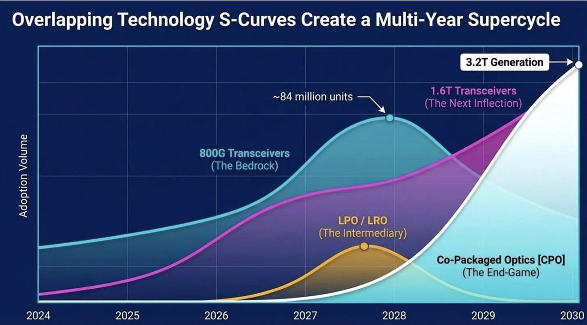
$SIVE Sivers Semiconductors: The Photonics Inflection In the semiconductor world, real alpha is found where physics hits a wall. Today, that wall isn’t GPU compute power - it’s interconnect bandwidth. As we transition to 1.6T networking, copper is dying, and light is taking over. Sivers Semiconductors ($SIVE) is no longer just a "Swedish tech hope." It has officially transitioned from an engineering research house to a high-volume product company. 1⃣ The 1.6T AI Bottleneck: Indium Phosphide (InP) AI clusters are only as fast as the links between them. Silicon Photonics (SiPh) is the solution, but silicon cannot emit light efficiently. It needs an external "engine." ➡️The Moat: Sivers is one of the few global players capable of mass-producing InP CW-WDM laser arrays. These are the "spark plugs" for the next generation of AI transceivers. ➡️Proof of Concept: Partnership with $POET is hitting a critical milestone. Prototype External Light Source (ELS) modules for 1.6T architectures are sampling in H1 2026. ➡️The Pivot to "Standard Products": CEO Vikram Vathulya recently confirmed a strategic shift. Sivers is moving away from low-margin custom engineering toward Standard Products. This will drastically shorten "time-to-revenue" and scale margins by serving multiple customers with the same high-spec chips. 2⃣ Hard Evidence: The 2026 Contract Ramp-up Investors have long criticized Sivers for a "paper pipeline." That changed this month (March 2026): ➡️LiDAR Breakthrough: A strategic LiDAR customer (winning in both Automotive and Industrial) is ramping up in Q4 2026. Cumulative revenue potential: $53M to $138M. ➡️SATCOM & IRIS² Momentum: The Wireless division grew 33% in 2025 (constant FX). Crucially, three terminal vendors for Europe's IRIS² satellite constellation have moved to the RFP stage and are currently building prototypes using Sivers technology. ➡️US Chips Act: Sivers is using Chips Act funding not just for cash, but to accelerate the integration of their tech into US Defense "Electronic Warfare" (EW) programs. 3⃣ Financial De-Risking & The "Uplisting" Catalyst The biggest drag on $SIVE has been its balance sheet. That drag is being cut: ➡️Debt Refinancing (Feb 2026): Secured a $17M facility from Bootstrap Europe, consolidating all debt and providing a clear runway to the Q4 2026 ramp-up. ➡️The 2027 Line in the Sand: Management has set a firm target to reach full break-even/positive cash flow by the end of 2027. ➡️The US Nasdaq Spin-off: With 80% of Photonics revenue coming from the US, the plan to spin off Sivers Photonics into a US-listed entity remains the primary "valuation unlock" to capture US-style multiples (think Lumentum or Coherent). 4⃣ 2026 Guidance: The Roadmap to Pavement ➡️Opportunity Pipeline: Stands at $453M (up 64% YoY). ➡️Profitability Pivot: Q4 2025 delivered a positive Adjusted EBITDA of $1.14M. Expect this to stabilize as "Foundry Customers" (SME base business) provide a recurring revenue floor while waiting for the "Big Elephants" (AI & Auto) to join. ➡️OFC Los Angeles (March 15-19, 2026): Currently underway. Industry leaders are vetting Sivers' laser arrays. Success here is the catalyst for large-scale datacenter deployment. 👇Final Verdict Sivers is no longer a "story" stock; it is a "delivery" stock. As 1.6T networking becomes the standard for AI datacenters, the demand for Indium Phosphide laser sources is set to explode. Sivers is one of the very few companies sitting on the right IP at exactly the right time. What’s your take on the Silicon Photonics race? Are you betting on the massive, vertically integrated giants like Broadcom, or do you see the "pick-and-shovel" specialists like $SIVE capturing the real alpha in the 1.6T transition? Drop a comment below with your thoughts or ask me anything. I'm here for you. #Investing #Semiconductors #AIInfrastructure #StockPicking #Sivers #Photonics


我现在订阅数已经有32.5K啦! 真的超级感谢大家! 照这个速度下去,我简直不敢相信自己快要超过马斯克,变成X上订阅人数第的大佬了?! 特别感谢中文圈小伙伴们最近的力挺。当然啦,也必须要感谢日韩圈的朋友们从开始就路支持我!


I don't post dollar amounts because they don't matter. What matters is return %. Speaking of that... YTD: 3840.39%. I'm probably the only one in the world. Who called out multiple names that 10x'd in a short timeframe. Do you remember these thesis anon? 1. $AXTI 2. $SIVE 3. $AAOI 4. $LITE 5. $IQE 6. $AEHR 7. $CRCL 8. $EWY 9. Unimicron 10. Nitto Boseki 11. $OSS 12. $GDRZF 13. $RPI 14. $SOI 15. $ALRIB 16. $SNDK 17. $SIMO 18. $VPG 19. $TSEM 20. $ARM 21. $MRVL 22. $INTC 23. $LPK 24. $NBIS 25. $MU They're all up 100-1000%+, because... 1. I post a thesis. 2. People can see how the stock performs months later. 3. They turn out right (thesis validation) because they're up hundreds of percent + hold their returns. I really dislike the traditional X influencer who shows large dollar amounts or fancy watches/cars/private jets. Then use that to get more by selling expensive subscriptions rather than through market returns. So trying to set a new trend off pure information discovery/synthesis from free thesis posts and the results that follow in terms of return percentages. TLDR: Market returns in terms of percentages matter the most to validate a thesis. Not the dollar amount made.