Silicon Sorcerer

4.4K posts

Silicon Sorcerer banner
Silicon Sorcerer

Silicon Sorcerer

@hackradios

Startup founder making silicon photonics and ASICs.

Katılım Eylül 2017
239 Takip Edilen200 Takipçiler
Lawrence Whittaker
Lawrence Whittaker@ListerLawrence·
I’m not knocking John Ive as a designer, but I have just spent the last 20 seconds coming up with this….
Lawrence Whittaker tweet media
English
100
22
550
52.3K
Silicon Sorcerer
Silicon Sorcerer@hackradios·
@bensen So is that why it looks like a budget car with a tiny screen from 10 years ago?
English
0
0
0
321
Silicon Sorcerer retweetledi
Melian Refugee
Melian Refugee@escapefrommelos·
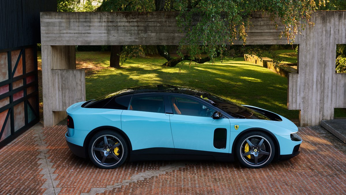
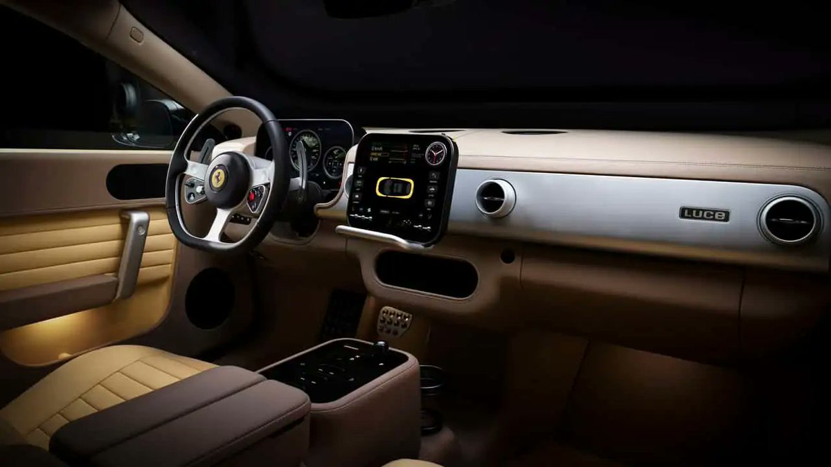
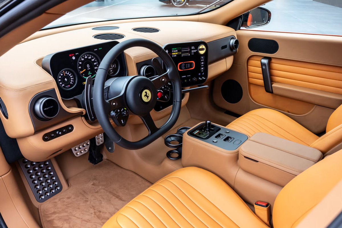
the remarkable thing about this “Jony Ive Designed EV Ferrari” is how dated it already looks, even the “smart” interior like a budget compact car from 2010, or a Chinese economy EV from five years ago
English
59
14
864
50.4K
EVCircles
EVCircles@EVCircles·
Surely the interior of the Ferrari Luce is lovely though, right? 😦 Oh… Maybe this is why we shouldn’t let non-car designers do cars?
EVCircles tweet media
English
49
1
95
6.2K
Jason Shuman
Jason Shuman@JasonrShuman·
People said the cyber truck was ugly when it first came out too…
English
98
1
29
7K
Silicon Sorcerer
Silicon Sorcerer@hackradios·
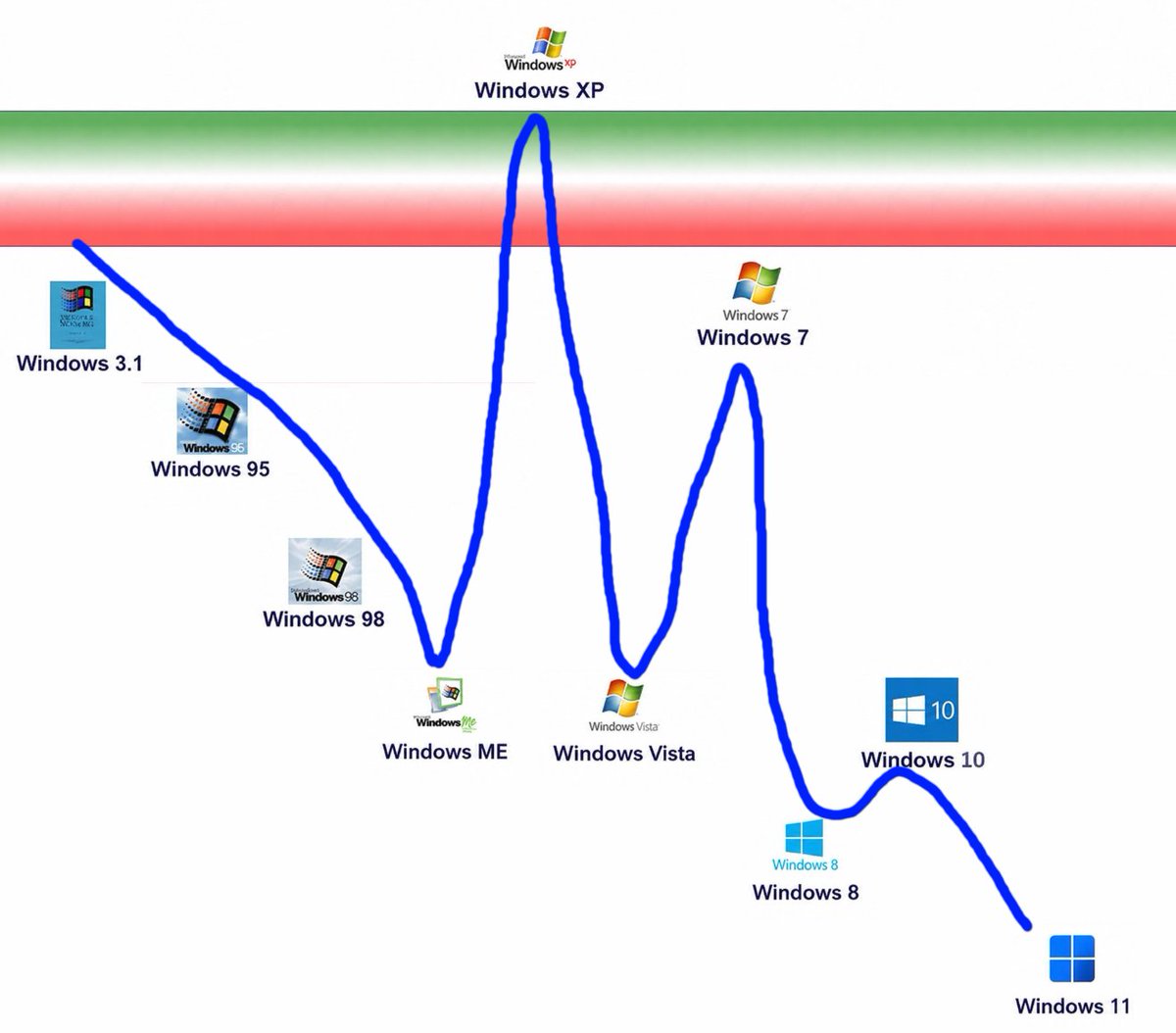
@m6502 Nah, Windows Vista stretches down into a bottomless pit. Those who were there know.
English
0
0
0
0
Silicon Sorcerer
Silicon Sorcerer@hackradios·
@SawyerMerritt Well it's quite apparent that the exterior was not co-designed with Jony I've. This thing is to a Ferrari what a Mustang Mach E is to a Mustang.
English
0
0
1
350
Sawyer Merritt
Sawyer Merritt@SawyerMerritt·
Ferrari has just officially unveiled its first ever all-electric car, called the Ferrari Luce. • Starting price: $640,000 • Interior co-designed with Apple's former head of design, Jony Ive • Range: 280 miles (expected EPA) • Peak charging speed: 350kW • 122 kWh battery • 1,050 horsepower • 0-60mph: 2.4s • 800v • Four-door four-seater • Four electric motors • OLED screens • Weight: 4,982 lbs • Front motors spin to 30,000 rpm, rears hit 25,500 rpm • Car uses an accelerometer to capture real vibrations from the electric motors & rear chassis. An algorithm filters out unpleasant frequencies and amplifies only the more “musical” sounds. This can be heard inside and outside the car. • Paddle shifter on steering wheel changes how aggressively torque is delivered, with five different levels • The trunk has 21.1 cubic feet of space, the largest luggage capacity the company has ever offered • 197.6 inches long, about as long as a Tesla Model S U.S. deliveries start in Q2 2027. More photos in the thread below:

Sawyer Merritt tweet mediaSawyer Merritt tweet mediaSawyer Merritt tweet mediaSawyer Merritt tweet media
English
5.7K
1.1K
9.7K
7.6M
墙街研究猿_The Ape of the Great Wall
让AI给我解释了一下: 传统芯片升级(摩尔定律)的“老路”是这样的: 想让芯片更快、更省电、塞更多晶体管 → 必须把晶体管画得越来越小(从10nm → 7nm → 5nm → 3nm → 2nm……)。 “画”这么小的线条,只能靠超级贵、超级难的光刻机(尤其是EUV极紫外光刻机)。 
每下一代节点,光刻机都要升级,成本爆炸(一台EUV光刻机上亿美元),设计预算也上10亿刀。 
华为以前被卡脖子,就是卡在这里——拿不到最先进的光刻机,就没法继续“横向缩”。 LogicFolding完全换了一条赛道: 它不缩小晶体管,而是把同一代工艺(固定节点)的电路,像折千层饼一样竖着叠起来! 还是用原来的晶体管大小(不需要新光刻机去画更小的图案)。 把关键的逻辑电路、内存、模拟电路拆开,一部分放在上层硅片,一部分放在下层硅片。 用超级密的“垂直电梯”(混合键合,1.5微米间距)把上下层直接焊在一起。 结果:信号走直达电梯,不用在平面上绕远路 → 线短了30%,RC寄生小了,频率更快、功耗更低、密度更高。
墙街研究猿_The Ape of the Great Wall tweet media
中文
67
47
306
138.8K
Silicon Sorcerer retweetledi
sdmat
sdmat@sdmat123·
The major players are perfectly capable of stacking silicon, and they use stacking in SOTA products (e.g. AMD V-Cache). However, they don't do fine-grained logic stacking - "folding" in Huawei's terminology. The reason for this isn't because the concept didn't occur to anyone; there is published research on exactly this technique going back a couple of decades. It's because moving to a smaller process node is a better option if you need more transistors. Two reasons: 1) Dissipating power from a single layer of logic is hard enough; dissipating it from a second layer through the first layer is a major problem and constrains achievable power density. 2) It's very expensive - silicon area scales directly with the number of layers, and it adds manufacturing steps and defect sources. Moving to a better process gives not just area reduction / density improvement but also better power and performance characteristics. So it's an easy choice. What is actually going on here is that Huawei doesn't have this choice available to them and is trying to spin a necessity as a virtue. For the rest of it, the industry already has a name for "optimize across device, circuit, chip and system rather than just shrinking transistors": STCO (System-Technology Co-Optimization). It is bog standard practice. Node progress is slowing down, and eventually fine-grained logic stacking will be more appealing. But right now it is a crutch.
Huawei@Huawei

HUAWEI has presented the Tau (τ) Scaling Law, a new principle for guiding the future development of the semiconductor industry. By 2031, HUAWEI's high-end chips based on this law are expected to feature a transistor density that is equivalent to 14 Å (1.4 nm) processes.

English
5
3
55
14.2K
Silicon Sorcerer
Silicon Sorcerer@hackradios·
@bubbleboi No dude they invented a new logic optimization technique that nobody else can use! They're going to take the lead while we keep fiddling with our EUV gadgets!!!
English
1
0
1
277
ALIENWARE
ALIENWARE@Alienware·
Introducing a streamlined 15” with a 15.3” 165Hz display. Pure gaming efficiency. @Intel
English
11
2
72
1.1M
Silicon Sorcerer
Silicon Sorcerer@hackradios·
@jukan05 Do you really think Huawei invented some sort of CMOS logic optimization trick that nobody else can implement or isn't already implementing? Come on...
English
0
0
0
341
Jukan
Jukan@jukan05·
Huawei's latest announcement carries real significance, because China has, in effect, shown the direction in which advanced technology needs to move. And it has done so in cutting-edge semiconductors, no less. China has long been a follower. In semiconductors, Western technology played the role of the pioneer, while China was preoccupied with simply keeping pace. But by banning EUV exports to China, the U.S. manufactured a bottleneck at the lithography tool — and in doing so, it effectively forced creativity onto China. To circumvent the sanctions, China was pushed toward approaches the West had never needed to take. That is exactly what today's announcement represents. Where Nvidia co-designs memory, packaging, and logic to optimize TCO at the system level — doing it rack by rack — Huawei is doing the same thing at the chip level. I'll say it again: this is a genuinely striking approach. Memory makers are already struggling with cost scaling. As linewidths shrink, the resources required to keep shrinking them — capital, manpower, time — are climbing exponentially. So the day will come when the West, too, must make packaging, logic, and memory collaborate from the node-design stage. And it won't be far off. China, through the paradox of sanctions, has been driven to do this ahead of the West — unintentionally. This is what genuinely frightens me. As YMTC has already demonstrated, U.S. sanctions pushed China to skip the incumbent standard and jump straight to the next-generation one. The result? YMTC carved out a meaningful presence in hybrid bonding — and even Samsung, the king of NAND, ended up licensing YMTC's patents. I believe the West may well find itself licensing this Huawei technology a few years down the road. And I believe cases like these will multiply, spreading China-style standards in their wake.
Jukan tweet media
English
71
211
1.1K
286.2K
Silicon Sorcerer
Silicon Sorcerer@hackradios·
@zephyr_z9 Can someone please explain to me exactly what this is and why companies with access to the latest process from TSMC/Intel wouldn't already be applying these logic optimizations to their own designs?
English
0
0
0
304
Zephyr
Zephyr@zephyr_z9·
Guess the easter egg, anon?? Hint: Why is there a huge jump in density from 2030 to 2031
Zephyr tweet media
English
20
11
305
54.7K
Silicon Sorcerer
Silicon Sorcerer@hackradios·
@PhotonCap Horrible AI slop that's wrong on so many levels. There is nothing worth understanding in this cartoon.
English
0
0
1
40
Mustafa
Mustafa@oprydai·
engineering is beautiful
Mustafa tweet media
English
13
39
852
17.4K